
This article described how to add the protection circuit to 18650 battery the CORRECT WAY and how I build my own battery charger and an IoT power supply subsystem which consists of a battery charger, a 3.3v/5v boost/buck converter with very low quiescent current.
18650 Battery and Battery Protection
One of the common things that many makers do is salvage useful parts from discarded electronics. I'm no exception, one of the parts that I salvage is 18650 Li-Ion battery, I have collected quite a few of them. 18650 is great and useful for battery-powered devices and my IoT projects, but they do not come with the built-in protection circuit like many of Li-Po battery packs do.
The 18650 Li-Ion battery is great, with its "standardised" size of 18mm diameter and 65mm long, and miltiple manufacturers (such as LG chemical, Samsung, Panasonics and Sony/Murata), make it very versatile for various applications, ranging from vaccuum cleaner robots, torch lights to many home-appliances and IoT devices. However, it does not come with any build-in protection circuit like commonly seeing in the Li-Po battery packs.
One of a Li-Po/Li-Ion battery protection circuit widely available consists of a DW01 and a pair of MOSFETs. It requires chip such as DW01 to provide undervoltage-lockout (UVLO) when the battery voltage drop to certain level to cut-off the battery from the load, so that the battery will not be permanently damaged due to over-draining the battery.
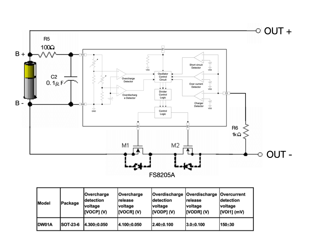
There are many DW01 chips from various Taiwan and Chinese vendors, all are similar yet slightly different. Check the datasheet of the chip you are actually used and test it against various specifications before production. The parameters on the block diagram are based on DW01A from Fortune Semiconductor - a Taiwan-based chip vendor.
In DW01 terms, the UVLO is called Over-Discharge Dectection Voltage (VODP) which is set to 2.4v+/-0.1 volts. If the battery drop to this voltage, it will turn off the M1 N-ch MOSFET, which will disconnect the battery from the load. The M1 will not be turn on again until the battery is charged and reach to Over-Dischange Release Voltage (VODR) 3.0+/-0.1 voltage. Together with M2, it allows current to flow from the battery to the load. The resistor R5 and cpacitor C2 surpress the ripple and disturbance form the charger and improve the ESD performance(the larger the value the better ESD performance), it typically using 100 ohm value, but I've seen design with 470 ohm or even 1k ohm.
The DW01 also provides Charging Detection, Short Circuit/Over-Current Detection by sensing the current flow through the resistor R6. The charging detection is achieved by comparing the voltage drop across R6 with the battery voltage to determine whether it should turn on or turn off the M2 MOSFET. When a discharged battery is connect to the charger, the charger will be in trickle-charge mode with a trickle current of 130mA until it reached to 3.1V. In some case where the battery voltage is below the discharged protection voltage of 2.4V is connected to the charger, the DW01 might not be able to detect the charging condition, the DW01 datasheet has an interesting footnote to kick-start the trickle-charge that many people failed to see:
Note: When a battery is connected for the first time, it may not enter the normal condition (dischargeable may not enabled). In this case, short the CS and VSS pins or connect to a charger to restore to the normal condition.
The CORRECT WAY for 18650 Battery Protection
The DW01 together with the pair of MOSFETs protection circuit only work properly IF the DW01 and the MOSFET are PERMANENTLY attached to the battery (like what you see in a Li-Po battery pack where the protection formed a unseparatable/permanent part of the battery). In case of 18650 battery, try to imagining that you charged the battery, take it out of the charger battery holder, and put it in a torch light, or plug it into your DIY electronic project, the battery is no longer attached to a battery protection circuitry, so the battery could drain way below 2.4V. If you have a short circuit in your electronic project, there is no R6 there to detect the over-current to offer the short circuit protection. Furthermore, the charger you used may or may not provide the battery charging protection circuit (more on that later), and the charger could keep charging the battery in constant voltage mode.
So the correct way to use 18650 battery is to attach it with the battery protection circuit permanently.
There are DW01+MOSFET module in a circular PCB that you could purchase from places like Aliexpress and retrofited it to the 18650 battery like showing in the picture below.
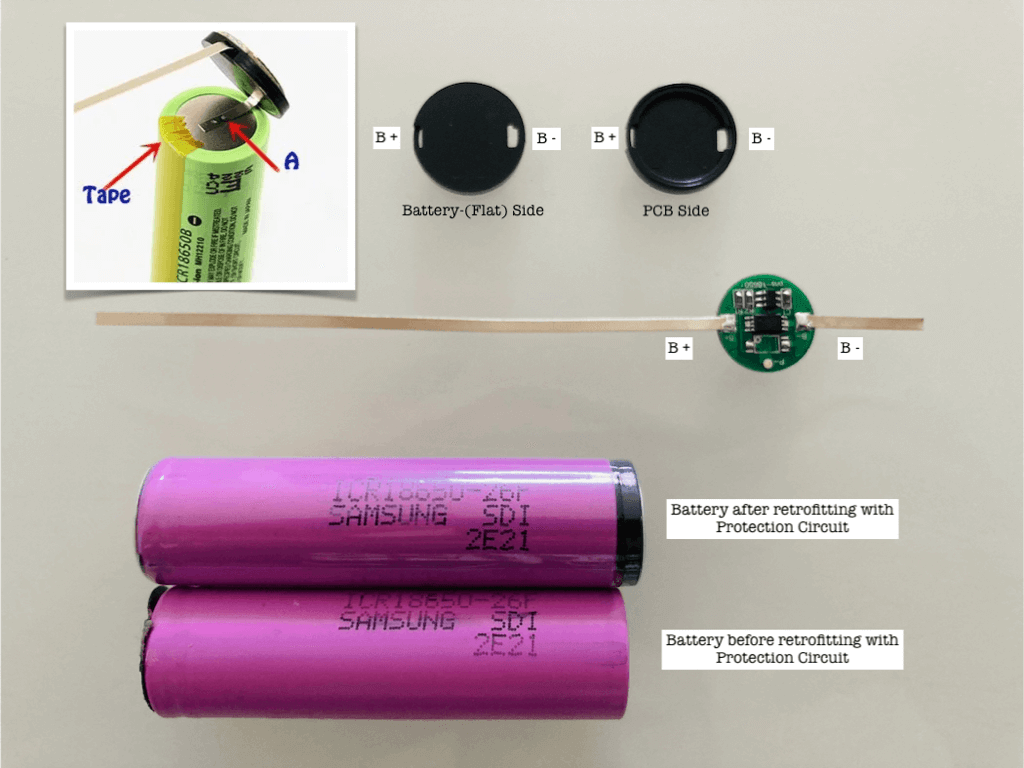
With this modification, it provides:
- Under-voltage Dischage Proection at 2.4V
- Over-charge Detection at 4.3V
- Short circuit/Over-current Protection (Over-current Detection Voltage 150mV)
- Reverse Polarity Battery Protection
This is what I did for every one of my 18650 batteries. This added about 3mm to the overall length of the battery, and a typical 18650 battery holder would not (or barely) fit the modified 18650 battery, which is one of the reasons (but not the only reason) that prompt me to design my own battery charger (with custom battery holder).
Design Goals
There are several other reasons that I want to designed my own 18650 charger or generic Li-Ion/Li-Po charger. One of a goals this year for me is to transit everything from USB A or USB micro to USB C, my old charger on a protoboard needs an upgrade. In the past several years, I found myself repeatively incorporating battery charging circuit, load sharing circuit again and again in my various IoT projects, it will be nice to separate the battery power management and charger into a Battery Power Management sub-system. The Li-Ion/Li-Po battery voltage varies between 2.4 to 4.2V, and many of the MCU can only work up to 3.6V, so some sort of Boost/Buck converter would need and it would be good to add it into this sub-system too, and whatever Boost/Buck converter would need to have low quiescent current for IoT project.
The design goals:
- On-board 18650 battery holder able to fit standard 18650 and modified one;
- USB Type C power input port;
- Capable to charge either 18650 battery and Li-Po battery (via JST connector);
- Battery Protection for 18650 battery;
- Load-sharing circuitry so it can power the load while charging;
- Boost/Buck converter capable to deliver 500mA power with either 3.3V or 5V output;
- Low quiescent current for IoT application.
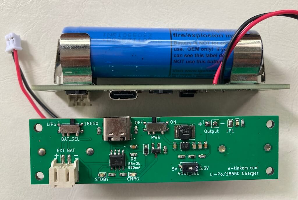
So here is the design that I come up with:
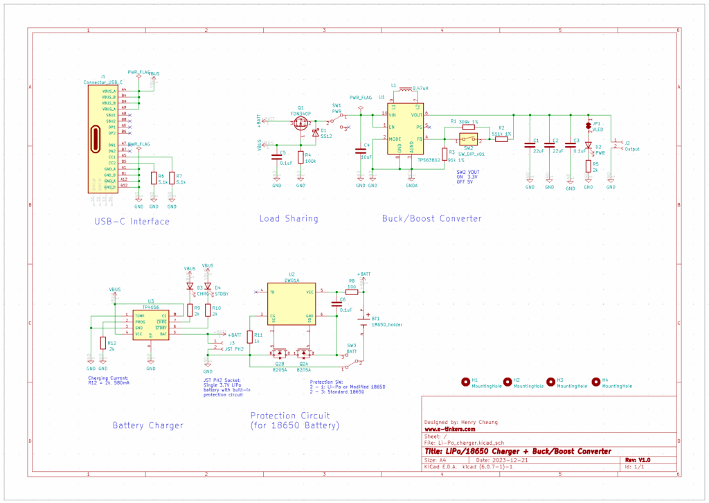
Charging Circuit
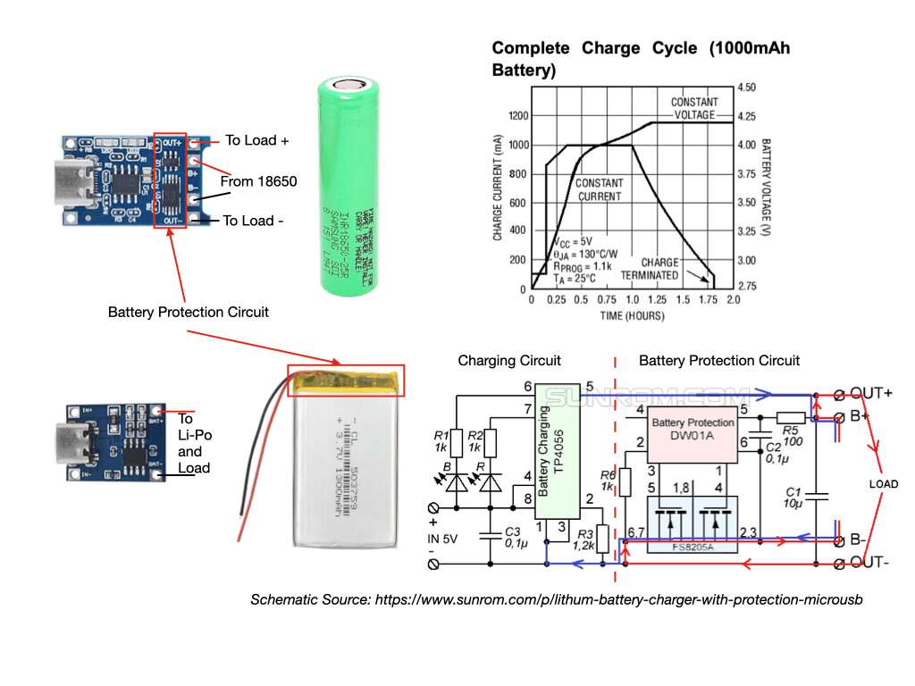
TP4056 from Nanjing Top Power is widely available and popular because there are readily-made module with or without battery protection circuit that can be purchased from places like Aliexpress and Amazon that costs $1-2 for 10 pieces, there are two type of TP4056 modules available in the market, one with the protection circuit that consists of DW01 and Dual MOSFET FS8205A. They are designed for different type of batteries, for example, for 18650 which does not have battery protection circuit build-in into the batttery, the TP4056 with extra protection chips should be used, but for those Li-Po battery which usually have its own protection circuit wrapped within the Kepton tape on top of the battery pack, there is no need for extra protection circuit, and the TP4056 module without the protection circuit should be used.
My design is very much similiar to those modules, the switch SW3 in my circuit is used to switch-in and switch-out the battery protection circuit for different type of batteries. At any giving time, only one battery should connect to the charger, either via the JST connector J3 for Li-Po battery or 18650 battery via the battery holder. The battery holder can accomodate either the standard 18650 battery or the modified 18650 with protection circuit. When the SW3 is in position 1 (Li-Po), it bypass the protection circuit for Li-Po/modified 18650 battery; for standard 18650 battery, SW3 needs to be in position 3(18650).
The TP4056 works in such a way that if the battery to be charged is below 2.9v, it will operates in trickle-charge mode with 130mA. When the battery get charged to 2.9v, it will enter the constant current mode, and charging current is set by the R12 as shown in my schematic. The charging current is set by the value of R12 which has a value of 2k, and based on the TP4056 datasheet, the charging current would be 580mA when the charging is in constant-current mode. This works for most of my batteries which are all above 1000mAH, and the battery should be charged at roughly half of its capacity C (1000mAH), 580mA is slightly higher than 1000/2. R12 value can be set higher for battery higher than 1000mAH. The constant-current mode will remain until the battery is charge to about 4.1v, it will then enter the constant-voltage mode and the charging current will start to decrease gradually until it reached the cut-off current threshhold. The resistor value of R12 is not only control the battery charging current, it also determine the cut-off of charging when the charging current drop to 10% of the constant-current. So if the charging current is set to 580mA, the cut-off current threshhold would be 580/10 = 58mA.
Load Sharing
The cut-off current threshhold protect the battery from overcharging but it create a potential problem if you connect the charger and battery to a load (e.g. an MCU board) while charging. If the load is drawing current less than 58mA (which is 10% of the constant charging current), then it not much a problem and the battery will be protected from overcharging when the charging current drop to below 58mA. However, if the load consumed more than 58mA, say 100mA, the charging current will not be able to drop to 58mA due to the load, the charging will continue and never end.
Microchip has an Application Note talk about Designing A Li-Ion Battery Charger and Load Sharing System and my load sharing design is based on the application note. When USB power is not plug in, the pull-down resistor R4 pull the gate of the P-Ch MOSFET (Q1) to zero allowing current to flow out of the battery to the load. When the USB power is plug-in, the gate of Q1 is high, and the MOSFET is off. With Q1 off, battery is cut-off from the load, allowing charging the battery without the load. At the same time, the power from the USB power source is powering the load via D1. This is one of the design feature of all the 18650 Charger/UPS module lack of (or wrong design mistake) that I found available in Aliexpress/Amazon.
Boost/Buck Converter
True to be told, I have never done a boost/buck converter design myself before, I don't quite like boost/buck converter even though switching power supplies have high efficiency, but they are noise and difficult to design properly, and if you are using ADC, you don't want the noise go into the power rail of ADC circuit and causing the reading to flutuate due to the EDS picked from the supply. However, boost/buck converter is really convenience when you think of powering IoT project using a Li-Po/Li-Ion battery. The voltage of the battery can varies from anywhere between 2.4V to 4.2V, where the MCU requires either 5V or 3.3V, and most of the 3.3 devices can't operates higher than 3.6V, so some sort of regulator would be required. The 3.3V linear regulator would requires an input voltage at least around 3.5V, so it is not very effecient to take the full advantage of Li-Po/Li-Ion batteries. So in this project, I decided to give it a try.
One of the design consideration is the quiescent current of the chip has to be as low as possible, when an IoT product go into deep sleep mode, the quiesent current of the power supply as well as the IoT chip's quiescent current would determine how long a battery could last. After some search, I decided on TPS63802 from Texas Instruments. it capable to deliver output of 1.3-5.5V @2A maximum output, with very low quiescent current of 11uA.
As the chip has really tiny VSON package of 3mm x 2mm, instead of build a custom PCB to test out the chip, I decided to search on Aliexpress to see if I could find a break out board, and I'm quite happy that I found one.
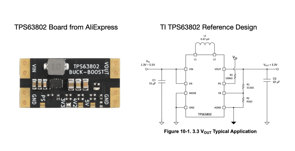
I ordder the board with 3.3V output, the board came with the jumper on the 3V3 pads joined by the solder. This board can configured to have output as 3V3, 4V2 or 5V by soldering the related jumper pads while keep others open. I remove the resistor that connect to the Power indication LED, so that I can measure the true no-load current consumption. With such as simple board with only a few components, what can go wrong? It turn out, there are several design faults, so never trust the design purchased from AliExpress-alike until you reverse-enginnering the circuit and conduct your own measurements.
To simulate an input Li-Ion battery, I apply various input voltage between 2.4V to 4.2V to the boost/buck converter, to my surprise, the no-load current are quite high at 6mA to 19mA at various input voltage. The board has a few differences from TI's reference design:
- The MODE pin, instead of connecting to the GND for Power Saving mode, but by default, it connected to a 10k-ohm pull-up resistor to Vin;
- There is a jumper pad on the board that marked as PS which allows to connect the MODE pin to the GND;
- The pull-up resistor on PG pin (R3 on TI reference design) is 10k-ohm instead of 100k ohm as susggested by TI's reference design;
- The R1 value for 5V output is different from datasheet's suggested value;
- There are more decoupling capacitors on both input and output to improve the ESD performance.
According to datasheet, the PG pin is an open-drain output for Power Good driver, and can be "leave (the PG pin) unconnected when not used". Although the board can be configured to PS mode by shorting the PS jumper to ground, but this literally connect the 10k-ohm pull-up resitor between Vin and GND, and therefore a pure leakage of Vin/10k current for no obvious reason. By removing the Pull-up resitors on both MODE and PG pins, the no-load current dropped from +400uA to about 20uA, this is still higher than the datasheet's 11uA, but close enough. I couldn't figure out what else could caused a few uA leakage unless it was caused by those decoupling capacitors. Adding back the Power indication LED incerase the current from 20uA to 500uA.
One interesting thing that I found out from the datasheet is that in order to generate a 5V output, the value of R1 on TI's reference design according to the formula should be 819k-ohm instead of the value given in the table 10-5 of the datasheet as 806k-ohm.
R1 = R2 x (Vout/Vfb - 1) = 91000 x (5/0.5 - 1) = 819000ohmMeasuring the board confirmed that the datasheet's 806k-ohm is wrong, this is one thing that the AliExpress board did correctly as I measured approximately 820k-ohm which is inline with the calculation from the formula.
In order for the TPS63802 to operate properly, the voltage at FB pin need to be at 500mV, and this is achieved by R1 and R2 value on the reference design. Based on the Aliexpress board design, if for any reason the voltage selection jumper pads on the board is left open, the Vref will no longer at 500mV, and I test the board by limited the input supply current to 500mA, the output current is running at nearly maximum at 490mA without any load when none of the jumper pads for voltage selection is connected (i.e. when R1 on the reference design is not connected), this means that it is not a good idea to have R1 on the reference design disconnected, so in my design instead of using jumper pads for output voltage selection, I decided to have two resistors connected in series to form the R1, and use a DIP switch to short one of two resistors for selecting between 3.3V and 5V output voltages, this ensures that Pin FB is always has a reference voltage.
SW2 on my schematic diagram is the voltage selection DIP switch that I just mentined for selecting between 3.3V and 5V, when it is in th ON position, the output voltage will be 3.3V, and when it is in the OFF position, the output voltage is 5V. The Power Indication LED can be enabled by shorting the PCB jumper JP1, but in many cases in IoT project deployed in th field, we'd want the battery to last as long as possible and the Power Indication LED probably is not visible and consealed in a water-proof enclosure, in this case, keep the JP1 open would save around 0.5mA current drawed by the LED and reduce the over quiescent current to 20uA. SW1 is the power switch for turning on and off the battery power to the boost/buck converter.
Now I have a Battery Power Supply sub-system that I can used in any of my electronic projects that requires a battery and charge, and do not need to incorporate the circuit in the PCB design over and over again.
The PCB design files are available on my Github, feel free to make your own one.